
Decoding Material Magic: How New Light Reveals Secrets of Thin Films

"Unlocking the potential of organic electronics: New research uses photoluminescence to peer inside thin films, paving the way for brighter screens and flexible tech."
Imagine a world where your phone screen bends without breaking, solar panels are as thin as paper, and new technologies are not only powerful but also eco-friendly. Organic semiconductors, materials that combine the properties of both plastics and semiconductors, are making this future a tangible possibility. The key to unlocking their potential lies in understanding how light interacts with these materials at a molecular level.
Researchers are increasingly turning to photoluminescence spectroscopy (PL), a technique that involves shining light on a material and analyzing the light it emits. This emitted light acts like a fingerprint, revealing crucial information about the material's structure, energy levels, and interactions between molecules. For materials like thin films, which are essential components in displays, solar cells, and flexible electronics, PL provides a non-destructive way to optimize their performance.
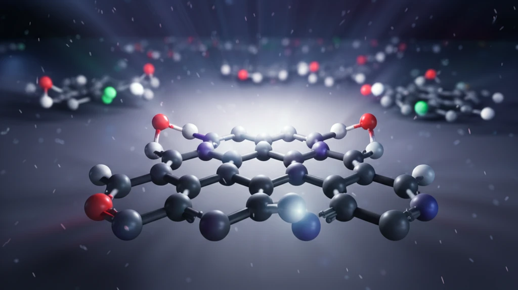
New research published in The Journal of Chemical Physics delves into the intricate world of thin films composed of pentacene (PEN) and perfluoropentacene (PFP), two organic semiconductors. By carefully analyzing the light emitted from these films, scientists are gaining insights into how these materials interact and how their properties can be fine-tuned. This article breaks down this complex research, making it accessible and exploring its potential impact on the future of technology.
Research Activity and Application Potential
Publication trends show growing scientific interest in organic semiconductor thin films and their processing methods across the literature. A 2025 study provided detailed optical characterization of 19 organic thin-film compounds on quartz glass and indium tin oxide substrates, revealing substrate-dependent behavior. Organic thin-film transistors have emerged as a feasible technology for flexible and wearable applications due to their biocompatibility, solution processability, light weight, intrinsic flexibility, low-temperature processing, and low cost.
Conventional Fabrication and Performance Constraints
Solution-processed thin-film devices — including transistors, memory, solar cells, OLEDs, thermoelectrics, sensors, and actuators — have been pursued for low-cost, scalable, vacuum-free fabrication routes. Organic semiconductors underpin flexible electronics, photovoltaics, and light-emitting diodes where nanoscale order and interfacial structure critically determine performance. However, organic thin-film transistors face a fundamental limitation: their sluggish response time stemming from slow carrier mobility restricts broader application despite valued transparency, flexibility, and low cost.
From Inorganic Dominance to Organic Emergence
For approximately fifty years, inorganic semiconductors such as silicon, gallium arsenide, and silicon dioxide insulators, alongside metals like aluminum and copper, formed the backbone of the semiconductor industry. Thin films — layers ranging from fractions of a nanometer to several micrometers — have long been a fundamental materials synthesis step across metals, semiconductors, oxides, polymers, and ceramics. Organic semiconductors, composed of π-bonded molecules or polymers of carbon and hydrogen (sometimes with nitrogen, sulfur, or oxygen), exist as molecular crystals or amorphous thin films, representing a distinct materials class from their inorganic predecessors.
Why Pentacene and Perfluoropentacene? The Perfect Pair for Organic Electronics
Pentacene (PEN) and perfluoropentacene (PFP) aren't just randomly chosen molecules. They're ideal candidates for studying organic semiconductors because of their unique compatibility. Think of them like LEGO bricks that fit together perfectly, even though they have slightly different shapes.
- Structural Compatibility: PEN and PFP have similar molecular geometries, allowing them to mix well and form stable thin films. This intermixing is crucial for creating materials with enhanced properties.
- Donor-Acceptor System: PEN and PFP exhibit different electron affinities, meaning one readily donates electrons (PEN), while the other readily accepts them (PFP). This donor-acceptor relationship is essential for creating efficient electronic devices.
- High Charge Carrier Mobility: Both materials are known for their ability to efficiently transport electrical charges, a key requirement for high-performance electronic devices.
Novel Structures, Nanostructuring, and Supramolecular Approaches
Recent work demonstrates an organic field-effect transistor gas sensor using a poly(3-hexylthiophene) film combined with functionalized porous carbon materials. Nanostructuring techniques are advancing to enhance charge mobility and luminescence efficiency, while sustainability concerns drive exploration of biodegradable organic electronics to address electronic waste. Covalent organic frameworks (COFs) are being systematically investigated for structure-property relationships and interface synthesis strategies, particularly as semiconductor active layers and dielectric materials in OTFTs. Kyoto University researchers have developed a pathway for structural analysis of supramolecular thin films, offering design guidelines for hydrogen-bonded transistors published in Angewandte Chemie.
Stability and Performance Bottlenecks
Despite advancements, organic electronics face persistent challenges: a 2013 review highlighted that performance of both p-type and n-type conducting polymers and small-molecule semiconductors remains primarily characterized by mobility and current on/off ratio limitations. N-type organic semiconducting polymers specifically suffer from ambient operational instability, a critical bottleneck for their use in organic thin-film transistors, organic electrochemical transistors, and organic thermoelectric devices. Research emphasizes synthetic methods to overcome these stability limitations, though the fundamental vulnerability of electron-transporting materials to environmental degradation remains a significant barrier.
Comparative Landscape
Organic thin-film technologies occupy a distinct niche compared to inorganic counterparts, trading peak carrier mobility and environmental stability for mechanical flexibility, solution processability at low temperatures, and potential for large-area, low-cost manufacturing. While inorganic semiconductors dominate high-performance computing and power electronics, organic thin films enable form factors — conformal, stretchable, transient — that are inaccessible to rigid crystalline materials. Direct performance comparisons remain context-dependent: metrics such as mobility, on/off ratio, and operational lifetime vary widely across material systems, device architectures, and encapsulation strategies, making blanket superiority claims inappropriate without specifying application requirements.
The Future is Bright: Toward More Efficient and Versatile Organic Electronics
The secrets hidden within organic semiconductor thin films are slowly being revealed through advanced techniques like photoluminescence spectroscopy. Understanding these materials at the molecular level is key to designing and creating next-generation electronic devices that are flexible, efficient, and sustainable. As research continues, we can expect to see even more innovative applications of organic semiconductors, transforming everything from our smartphones to our energy sources.
Optical Property Engineering via Molecular Interactions
A comprehensive 2025 review systematically investigated the fundamental principles, recent advances, and innovative strategies for modulating the optical properties of organic thin films through intermolecular interactions. The work emphasizes that controlling molecular packing, aggregation states, and interfacial energy transfer pathways enables precise tuning of absorption, emission, and waveguiding characteristics critical for optoelectronic applications.
Market Trajectory and Commercialization Horizon
Market analyses project robust growth for organic semiconductor thin films, with the OTFT segment alone forecast to reach approximately USD 1.5 billion by 2035 at a CAGR around 15% (2025–2035), while another estimate values the market at $1.8 billion in 2026 scaling to $6.14 billion by 2035 at 14.6% CAGR. The broader organic semiconductor market is segmented into OLED, organic photovoltaics, organic thin-film transistors, and others, with OLED accounting for the largest revenue share in 2025. Flexible display adoption in wearable devices is cited as a key driver as manufacturers pursue bendable electronics.
Materials Innovation and Ultrathin Regime Limits
Organic materials play a critical role in next-generation optoelectronic devices including organic solar cells, organic thin-film transistors, and OLEDs, with current research emphasizing materials design for these platforms. A fundamental challenge emerges at the ultrathin limit — films below 10 nm, comprising only several molecular layers — where carrier-transport regulation mechanisms change and solution-processed methods face significant hurdles in achieving uniform, continuous coverage and controlled morphology.
Societal Implications and Human-Centered Design
The transition toward organic thin-film electronics carries implications beyond technical specifications: biodegradable and biocompatible devices could reduce electronic waste and enable transient medical implants that dissolve harmlessly after fulfilling their function. Flexible, lightweight form factors promise wearable health monitors that conform to skin without discomfort, and conformable sensors that integrate into clothing or infrastructure. Realizing this potential requires not only materials breakthroughs but also supply-chain transparency, end-of-life recovery systems, and inclusive design processes that consider diverse user needs from the outset.