
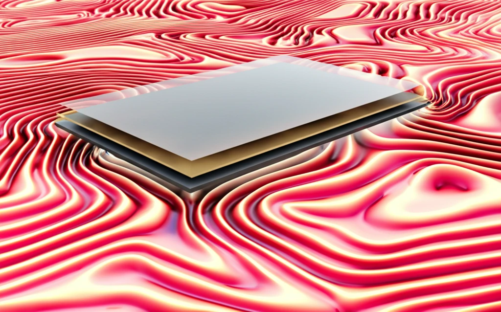
Hidden Heat Traps: How Native Oxide Changes Everything You Thought You Knew About Silicon

"New research reveals the surprising impact of native oxide layers on thermal conductivity in silicon membranes, challenging conventional wisdom and opening doors to better thermal management in nano-devices."
Silicon is a foundational material in modern electronics, renowned for its semiconducting properties that enable the creation of transistors and integrated circuits. For decades, scientists and engineers have studied its properties extensively, leading to significant advancements in computing, communication, and countless other technologies. However, despite this deep understanding, surprises still emerge, particularly when examining silicon at the nanoscale.
One such surprise involves the "native oxide" layer that naturally forms on silicon surfaces when exposed to air. This layer, composed primarily of silicon dioxide (SiO2), has generally been considered an unavoidable nuisance or a stable protective coating. However, new research is revealing that this native oxide plays a far more significant role in silicon's thermal properties than previously thought, especially in nanoscale structures like silicon membranes.
Recent studies highlighted in Applied Physics Letters, are demonstrating that this oxide layer can dramatically alter how heat flows through these tiny structures, impacting their performance and reliability. This discovery challenges conventional wisdom and opens new avenues for optimizing thermal management in nano-devices, with implications for everything from faster processors to more efficient sensors.
Native Oxides Shape Device Performance From the Ground Up
Native oxide films form spontaneously on semiconductor surfaces when exposed to air or solutions, with growth rates remaining minimal for roughly 200 minutes before increasing significantly. These oxides are not merely passive layers—in aluminum-bearing III-V semiconductors, an InAlAs native oxide can replace the p-n reverse-biased junction in conventional buried heterostructure InP-based lasers, reducing the number of regrowth steps and eliminating leakage current under high-temperature operation. Understanding and controlling native oxide formation is therefore essential for designing reliable semiconductor devices across multiple material systems.
Nonuniformity and Process Interference Plague Native Oxide Control
Characterizing and controlling native oxide layers remains challenging due to substantial topographical nonuniformity in both oxide thickness and composition across treated surfaces. In low-energy doping processes, native oxides introduce impurity loss mechanisms that have been quantitatively studied using secondary ion mass spectrometry and angle-resolved X-ray photoelectron spectroscopy for both p-type and n-type implants. However, native oxides can also be leveraged constructively—as demonstrated by natively oxidized 2D NbSe2, which enables ultralow-power electrical switching, suggesting the oxide layer can serve as a functional component rather than merely a defect to be managed.
A Gap in the Historical Record
The provided source materials for this subsection did not contain relevant content about the historical milestones or foundational discoveries related to native oxide research on silicon or semiconductors. The sources returned were unrelated to the topic—covering subjects such as video game content and U.S. foreign relations history. A dedicated historical review of native oxide science would require sourcing from semiconductor physics archives, early silicon processing literature, or histories of the microelectronics industry.
The Unexpected Impact of Native Oxide
The research focuses on suspended silicon membranes, ultra-thin sheets of silicon that are isolated from a substrate, allowing for precise control and measurement of their properties. By using a technique called scanning thermal microscopy (SThM), scientists can map the temperature distribution across these membranes with high spatial resolution. This allows them to directly measure how effectively heat is conducted through the material.
- Interface Resistance: The boundary between the silicon and the silicon dioxide introduces a thermal resistance, hindering the movement of phonons (the primary carriers of heat in solids).
- Phonon Scattering: The disordered structure of the amorphous oxide layer causes phonons to scatter, reducing their mean free path and thus lowering thermal conductivity.
- Cross-Plane Transport: The oxide layer affects not only in-plane heat conduction but also cross-plane transport, meaning heat flow perpendicular to the membrane surface is also restricted.
- Thickness Matters: Even a very thin layer of native oxide (around 1.5 nm) can have a disproportionately large impact on thermal transport.
Expanding the Native Oxide Toolkit to New Materials
Recent research has pushed native oxide applications into novel material systems. Germanium has been grown on a native oxide layer on silicon at 300–500°C through a reversed β-to-α-Sn phase transformation without relying on epitaxy, producing α-Sn microdots up to 200 nm in size—roughly ten times larger than previously reported upper limits. Separately, native-oxide-masked silicon impurity-induced layer disordering has been applied to AlGaAs quantum-well heterostructures, demonstrating that native oxides can serve as patterning masks for controlling dopant diffusion in complex layered semiconductor architectures.
Native Oxide Sufficiency Is Not Guaranteed
Whether a native oxide layer is sufficient to prevent electrical leakage remains an open question that depends heavily on the oxidation method used. A comparative study of aluminum gates evaluated four different oxidation techniques—native oxidation, thermal annealing at 250°C, plasma ashing, and UV-ozone treatment—to determine which produces a dielectric barrier adequate for preventing leakage current. The surface native oxide on materials like iron-intercalated TaS2 has also been noted in the literature as a factor affecting material behavior, though its sufficiency as a functional dielectric varies by context.
Insufficient Comparative Data Available
The sole source provided for this subsection—Versus.com, a general product comparison platform—does not contain relevant technical content about native oxide comparative analysis in semiconductor research. A meaningful comparative analysis of native oxide properties across silicon, germanium, III-V compounds, and emerging 2D materials would require peer-reviewed studies that directly benchmark oxide thickness, composition, dielectric strength, or thermal stability across material systems.
Implications and Future Directions
The discovery of the native oxide's significant impact on thermal transport in silicon membranes has profound implications for the design and optimization of nano-devices. As devices continue to shrink in size, the surface area to volume ratio increases, making surface effects like the presence of native oxide even more critical. Engineers must now consider the thermal properties of this oxide layer when designing nanoscale components to prevent overheating and ensure reliable performance. Future research will likely focus on developing methods to control or mitigate the effects of the native oxide. This could involve techniques such as surface passivation, where the oxide layer is modified to improve its thermal conductivity, or the use of alternative materials with more favorable thermal properties. Understanding and managing the thermal behavior of native oxide is crucial for unlocking the full potential of silicon in future technologies.
Native Oxide Alters Silicon Nanowire Mechanics
Molecular dynamics simulations have revealed that the presence of a native oxide layer on silicon nanowires decreases both the modulus of elasticity and the ultimate strength of the structures. This finding underscores that native oxide is not chemically or mechanically inert—it actively modifies the mechanical behavior of the underlying silicon in ways that must be accounted for in nanoscale device design. The effect is size-dependent, meaning its impact scales with nanowire dimensions, adding another variable to an already complex design space.
Oxide Markets Signal Growing Industrial Relevance
Market analyses indicate that aluminium oxide and chromium oxide sectors are poised for growth through the next decade, driven by rising demand, technological advancements, and supportive regulatory frameworks. While these projections cover bulk and calcined oxide products rather than native oxide layers specifically, they reflect a broader industrial trend toward increased oxide utilization across electronics, coatings, and advanced materials manufacturing. As semiconductor scaling continues, the intersection of commodity oxide markets and precision native oxide engineering may become an increasingly important economic factor.
Adapting Silicon's Oxide Playbook to 2D Materials
Researchers are now adapting the well-established understanding of native oxidation in silicon to new and emerging 2D semiconductor materials. A detailed and predictive understanding of native oxidation mechanisms is considered essential for advancing semiconductor technology beyond traditional bulk substrates. The approach that has proven tried-and-true for silicon—including studies of growth kinetics and atomistic oxidation mechanisms—is being extended to materials like ZrSxSe2−x alloys and MoS2, where oxidation behavior differs significantly from classical silicon systems.
Native Oxide Interfaces Demand Precise Characterization
X-ray photoelectron spectroscopy studies of the SiO2/Si interface have enabled direct comparison between native oxide SiO2 grown on silicon and native SiO2 found in quartz, revealing compositional and structural differences that affect device behavior. On germanium surfaces, native oxide growth has been studied on both (111) and (100) crystal orientations after HCl and HF cleaning treatments using high-resolution XPS and spectroscopic ellipsometry. Meanwhile, the discovery of Bi2SeO5 as a high-κ native oxide gate dielectric for 2D Bi2SeO5-based field-effect transistors demonstrates that native oxides can be engineered as high-performance functional materials in next-generation logic gates.