High-density GaAs nanowire array on silicon wafer

GaAs Nanowire Arrays: The Future of High-Density Electronics?

"Explore how substrate processing engineering is revolutionizing the creation of high-density Gallium Arsenide (GaAs) nanowire arrays, paving the way for faster, more efficient electronic devices."


In the relentless pursuit of smaller, faster, and more efficient electronic devices, scientists and engineers are constantly exploring new materials and fabrication techniques. Among the most promising developments is the creation of high-density nanowire arrays, particularly those made from Gallium Arsenide (GaAs). These arrays hold immense potential for revolutionizing various fields, from electronics to optoelectronics.

Nanowires, with their incredibly small dimensions (measured in nanometers), offer unique properties that bulk materials simply cannot match. When arranged in high-density arrays, these nanowires can dramatically enhance device performance, enabling faster processing speeds, lower power consumption, and increased sensitivity. However, creating these arrays is no easy task. It requires precise control over the growth and arrangement of the nanowires, often involving complex and costly fabrication processes.

Recent research has focused on a promising approach: substrate processing engineering. This method involves manipulating the surface of a substrate material to guide the growth of nanowires, allowing for the creation of high-density, vertically aligned arrays with remarkable efficiency. One such study, which we will explore in detail, demonstrates the successful fabrication of GaAs nanowire arrays through carefully controlled substrate etching and molecular beam epitaxy (MBE).

How Does Substrate Processing Engineering Work for GaAs Nanowires?

High-density GaAs nanowire array on silicon wafer

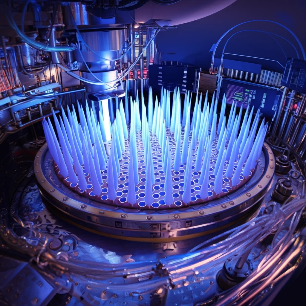
The key to this innovative approach lies in the precise manipulation of the substrate surface. Researchers used a technique involving diluted buffered oxide etch (BOE) to selectively etch silicon substrates. This etching process creates nanoholes on the substrate surface, which then act as templates for the growth of GaAs nanowires. The density and verticality of the resulting nanowire arrays are highly dependent on the concentration of the BOE solution used.

The process involves several critical steps:

  • Substrate Preparation: Silicon substrates are first cleaned to remove any contaminants.
  • BOE Etching: The substrates are then etched using diluted buffered oxide etch (BOE) at different concentrations. This step creates nanoholes on the surface.
  • Molecular Beam Epitaxy (MBE): GaAs nanowires are grown on the etched substrates using molecular beam epitaxy. This technique allows for precise control over the growth process.
  • Characterization: The resulting nanowire arrays are characterized using field-emission scanning electron microscopy (FE-SEM) to assess their density, verticality, and morphology.
The study found that the concentration of the BOE solution significantly impacts the quality of the nanowire arrays. An optimal concentration of 1:10 diluted BOE solution resulted in GaAs nanowire arrays with a verticality of 93.3% and a density of 290 × 106 cm-2. Higher or lower concentrations led to reduced verticality and density.

The Future is Small: High-Density Nanowire Arrays on the Horizon

The development of high-density GaAs nanowire arrays through substrate processing engineering represents a significant step forward in the field of nanotechnology. This method offers a cost-effective and scalable approach to creating advanced electronic and optoelectronic devices. As research continues, we can expect to see further innovations in nanowire fabrication techniques, paving the way for even smaller, faster, and more efficient technologies in the years to come. These advancements promise to transform various industries, from consumer electronics to renewable energy, making our devices more powerful and sustainable.

About this Article -

This article was crafted using a human-AI hybrid and collaborative approach. AI assisted our team with initial drafting, research insights, identifying key questions, and image generation. Our human editors guided topic selection, defined the angle, structured the content, ensured factual accuracy and relevance, refined the tone, and conducted thorough editing to deliver helpful, high-quality information.See our About page for more information.

This article is based on research published under:

DOI-LINK: 10.1088/2053-1591/aaf340, Alternate LINK

Title: High Density Gaas Nanowire Arrays Through Substrate Processing Engineering

Subject: Metals and Alloys

Journal: Materials Research Express

Publisher: IOP Publishing

Authors: Yubin Kang, Jilong Tang, Penghua Wang, Fengyuan Lin, Xuan Fang, Dan Fang, Dengkui Wang, Xiaohua Wang, Zhipeng Wei

Published: 2018-12-05

Everything You Need To Know

1

What is substrate processing engineering and how does it facilitate the creation of Gallium Arsenide nanowires?

Substrate processing engineering for Gallium Arsenide nanowires involves manipulating the surface of a substrate, often silicon, to guide the growth of nanowires. In one approach, diluted buffered oxide etch, or BOE, is used to selectively etch the silicon substrates, creating nanoholes that act as templates. The density and vertical alignment of the resulting Gallium Arsenide nanowire arrays are highly dependent on the concentration of the BOE solution.

2

How is molecular beam epitaxy, or MBE, utilized in the fabrication of Gallium Arsenide nanowire arrays, and what role does FE-SEM play in this process?

Molecular beam epitaxy, or MBE, is used to grow Gallium Arsenide nanowires on etched substrates. MBE is a technique that allows for precise control over the growth process at the atomic level. This is essential for achieving high-quality nanowires with desired properties, such as uniform size and composition. Characterization techniques like field-emission scanning electron microscopy, or FE-SEM, are then used to assess the density, verticality, and morphology of the resulting nanowire arrays.

3

How does the concentration of buffered oxide etch, or BOE, influence the characteristics of Gallium Arsenide nanowire arrays?

The concentration of the buffered oxide etch, or BOE, solution significantly impacts the quality of the Gallium Arsenide nanowire arrays. Research indicates that an optimal concentration, such as a 1:10 dilution, can result in arrays with high verticality (e.g., 93.3%) and density (e.g., 290 × 106 cm-2). Higher or lower concentrations can lead to reduced verticality and density, affecting the overall performance of devices utilizing these arrays.

4

Why are high-density Gallium Arsenide nanowire arrays considered a significant advancement in nanotechnology?

High-density Gallium Arsenide nanowire arrays are pivotal because nanowires possess unique properties at nanoscale dimensions that are unmatched by bulk materials. Arranging them in high-density arrays can dramatically enhance device performance, enabling faster processing speeds and lower power consumption. The method of substrate processing engineering offers a cost-effective and scalable approach to creating advanced electronic and optoelectronic devices, indicating a path to smaller, faster, and more efficient technologies.

5

Beyond fabrication, what are the potential implications and future directions for high-density Gallium Arsenide nanowire arrays in various industries?

While the focus is on creating high-density Gallium Arsenide nanowire arrays, the implications extend to various applications. These advancements can potentially transform industries ranging from consumer electronics to renewable energy, making devices more powerful and sustainable. Further research into nanowire fabrication techniques could lead to even more innovative applications and improvements in existing technologies. However, topics such as specific doping techniques, surface passivation, and integration with other materials are not detailed here but are important for real-world application.

Newsletter Subscribe

Subscribe to get the latest articles and insights directly in your inbox.