Electrons flowing across a graphene sheet

Electrostatics in 2D Materials: Why This Correction Matters for Future Tech

"A crucial update clarifies the behavior of electrons in atomically thin materials, impacting developments in transistors, sensors, and beyond."


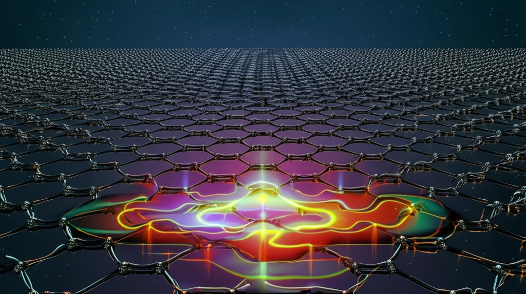
Imagine a world where electronics are even smaller, faster, and more energy-efficient than they are today. Two-dimensional (2D) materials, like graphene, are making this vision a reality. These materials, just a few atoms thick, possess unique electrical properties that make them ideal for use in advanced transistors, sensors, and other devices.

However, accurately predicting and controlling the behavior of electrons within these materials is essential for optimizing their performance. Electrostatics, the study of electric charges at rest, plays a critical role in this understanding. A recently published paper in the Journal of Applied Physics explored the electrostatics of lateral p-n junctions – the fundamental building blocks of many electronic devices – in atomically thin materials.

Now, an erratum (a correction) has been issued for this paper, specifically addressing an error in unit conversion that affected the calculated depletion widths. While this might seem like a minor detail, it has significant implications for researchers and engineers working with 2D materials. Let's break down why this correction is so important and how it impacts the future of technology.

What Was the Error and Why Does It Matter?

Electrons flowing across a graphene sheet

The original paper, titled “Electrostatics of lateral p-n junctions in atomically thin materials,” presented calculations and analysis of how electric fields and charges behave at the junction between p-type and n-type semiconducting regions within a 2D material. These junctions are essential for creating transistors and other electronic components.

The erratum addresses a unit conversion error that impacted the calculated depletion widths. The depletion width refers to the region within the p-n junction where mobile charge carriers (electrons and holes) are depleted, creating an insulating zone. The size of this depletion region directly influences the behavior and performance of the device.

  • Impact on Device Design: Accurate depletion width calculations are crucial for designing efficient and reliable devices based on 2D materials. An error in these calculations could lead to suboptimal device performance or even failure.
  • Understanding Electron Behavior: The depletion width is directly related to the distribution of electric fields and charges within the material. Correcting this error provides a more accurate understanding of electron behavior in these systems.
  • Reproducibility of Results: Scientific accuracy demands that published results are reproducible. The erratum ensures that other researchers can accurately replicate the findings of the original paper and build upon them with confidence.
Essentially, the corrected paper provides a more precise and reliable foundation for future research and development in 2D electronics. The original paper stated that the depletion widths were 10x larger than the proper values due to the unit conversion error. The corrected paper rectifies this mistake and provides accurate data

The Future of 2D Electronics: Smaller, Faster, and More Efficient

The ongoing research into 2D materials promises a revolution in electronics, driven by the unique properties and potential applications of these atomically thin structures. This correction to a critical scientific paper ensures that the foundation upon which this revolution is built is accurate and reliable, thus accelerating the innovation process. By refining our understanding of fundamental physics at the nanoscale, we pave the way for devices that are not only smaller and faster but also more energy-efficient and sustainable. As technology continues to evolve, 2D materials stand at the forefront of a new era of electronic possibilities, promising advancements that will transform industries and improve lives.

About this Article -

This article was crafted using a human-AI hybrid and collaborative approach. AI assisted our team with initial drafting, research insights, identifying key questions, and image generation. Our human editors guided topic selection, defined the angle, structured the content, ensured factual accuracy and relevance, refined the tone, and conducted thorough editing to deliver helpful, high-quality information.See our About page for more information.

This article is based on research published under:

DOI-LINK: 10.1063/1.5051548, Alternate LINK

Title: Erratum: “Electrostatics Of Lateral P-N Junctions In Atomically Thin Materials” [J. Appl. Phys. 122, 194501 (2017)]

Subject: General Physics and Astronomy

Journal: Journal of Applied Physics

Publisher: AIP Publishing

Authors: Ankur Nipane, Sirisha Jayanti, Abhinandan Borah, James T. Teherani

Published: 2018-10-07

Everything You Need To Know

1

What specific error was corrected in the research regarding electrostatics in 2D materials, and how did it affect the results?

The original paper on "Electrostatics of lateral p-n junctions in atomically thin materials" had a unit conversion error. This error led to incorrectly calculated depletion widths, with the original paper stating that the depletion widths were 10x larger than the proper values. The erratum corrects this mistake, providing accurate data crucial for designing efficient and reliable devices based on 2D materials.

2

In the context of 2D materials and p-n junctions, what exactly does "depletion width" refer to, and why is its accurate calculation so important?

Depletion width refers to the region within a p-n junction where mobile charge carriers, specifically electrons and holes, are depleted, creating an insulating zone. The size of the depletion width significantly influences the behavior and performance of devices built with 2D materials. Accurate calculation of the depletion widths is essential for the design and optimization of transistors and other electronic components.

3

Why is the correction to the published paper on electrostatics in 2D materials so critical for future research and development in electronics?

The correction to the paper is important for three key reasons: firstly, accurate depletion width calculations are crucial for the design of efficient and reliable devices based on 2D materials. Secondly, correcting the error provides a more accurate understanding of electron behavior within 2D materials. Finally, it ensures the reproducibility of the research findings, allowing other scientists and engineers to build upon the results with confidence.

4

What are 2D materials, and why are they considered promising candidates for revolutionizing future electronic devices?

Two-dimensional materials, such as graphene, are atomically thin substances with unique electrical properties, making them ideal for advanced transistors, sensors, and other devices. These materials hold the promise of electronics that are smaller, faster, and more energy-efficient. However, the behavior of electrons within these materials must be accurately predicted and controlled, and this is where the study of electrostatics becomes vital.

5

How does refining our understanding of electrostatics in 2D materials contribute to the broader vision of future electronics and technology?

The ongoing research into 2D materials, refined by corrections such as this erratum, paves the way for a revolution in electronics. By improving our understanding of fundamental physics at the nanoscale, we can develop devices that are not only smaller and faster but also more energy-efficient and sustainable. This area of research promises advancements that will transform industries and improve lives as 2D materials continue to evolve.

Newsletter Subscribe

Subscribe to get the latest articles and insights directly in your inbox.