
Unlocking the Secrets of Wear: A New Microscope Method Reveals All

"Scientists develop a revolutionary method using atomic force microscopy to measure and understand wear at the nanoscale, promising insights for everything from microdevices to materials science."
The world around us is constantly in motion, and with every interaction, materials experience wear. From the microscopic components of our smartphones to the massive gears of industrial machinery, understanding how materials degrade over time is crucial. Now, scientists have developed a groundbreaking new method to examine this process at the atomic level, using a technique called atomic force microscopy (AFM).
This innovative approach, described in a recent scientific publication, offers unprecedented insights into the mechanisms of wear. By measuring the minute changes in a material's surface, researchers can now gain a deeper understanding of the forces and processes that lead to degradation. This knowledge promises to revolutionize how we design and manufacture everything from tiny microdevices to large-scale engineering projects.
The key to this new method lies in its simplicity and precision. By focusing on the contact area between surfaces, researchers can determine the rate of material removal without relying on complex assumptions or specialized equipment. This opens the door to a new era of wear testing, one that's more efficient, accessible, and capable of revealing the fundamental principles governing material degradation.
Why Wear Matters
Wear affects the performance and service life of materials, components, and instruments, but its scale and mechanisms can vary widely. At very small dimensions, wear may be difficult to observe directly, making precise measurement important for understanding how surfaces change. The broader impact is therefore tied to the ability to quantify wear reliably across different length scales.
The AFM Measurement Challenge
Atomic force microscopy (AFM) is a standard approach for investigating wear at the nanometer scale, often by examining contact between an AFM tip and a surface. Researchers have also developed a six-degree-of-freedom topographical-difference method using large AFM measurements of up to 90 × 90 μm² to detect wear volumes. However, nanoscale wear rates can be low, while thermal drift makes quantitative wear-volume measurements demanding. Reviews identify scanning probe microscopy methods, including AFM and friction force microscopy, among the principal techniques used to measure nanoscale wear.
From Surface Imaging to Nanoscale Wear
The development of atomic force microscopy established a way to investigate wear mechanisms at the nanometer scale. Its use shifted attention toward controlled contact between an AFM tip and an interacting surface. This foundation enabled later methods designed to quantify wear volumes and examine wear across increasingly small length scales.
How the New AFM-Based Method Works: A Step-by-Step Guide
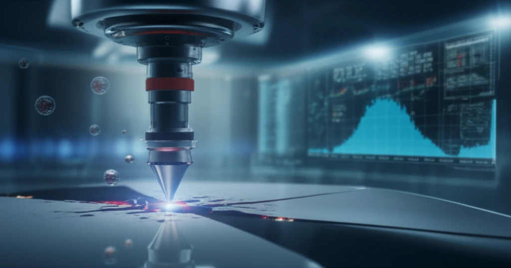
At the heart of this new method is the atomic force microscope (AFM), a powerful tool capable of imaging surfaces at the nanoscale. AFM works by using a tiny probe, essentially a microscopic needle, to scan across a surface. As the probe encounters features, it deflects, allowing researchers to create detailed maps of the surface.
- Scanning with the AFM: The AFM probe is used to scan the surface of a material, such as silicon, to measure the contact area.
- Measuring the contact area: The contact area is determined by scanning the worn probe against a sample with sharp spikes. This allows researchers to analyze the shape of the probe and determine how much material has worn away.
- Calculating the Wear Rate: Using this information, along with measurements of the probe's geometry, the researchers can calculate the rate at which the material is being removed.
Measuring Wear More Precisely
Recent work has focused on improving the quantification and tracking of wear from the micrometer to the nanometer scale. One approach uses large AFM topographical measurements and a six-degree-of-freedom comparison to detect wear volumes. A 2023 critical review surveys nanoscale wear measurement methods, including scanning probe microscopy techniques such as AFM and friction force microscopy.
Where Measurement Breaks Down
Nanoscale wear measurement remains challenging because wear rates can be very low and thermal drift can interfere with quantitative measurements. These limitations make it difficult to determine wear volumes accurately enough to establish reliable wear laws. The difficulty of predicting multi-asperity wear from first principles also reflects gaps in the ability to quantify and track wear across multiple length scales.
Two Mechanisms in Steel
A nanoscale wear characterization method was applied with an atomic force microscope to commercial AISI 52100 steel, a common bearing material. The reported experiments identified two wear mechanisms: atom attrition and another mechanism indicated in the study's results. This example shows how AFM-based analysis can distinguish nanoscale wear behavior in a specific engineering material rather than treating wear as a single uniform process.
The Future of Wear Research and Beyond
This new AFM-based method represents a significant step forward in the study of wear. By providing a simple, yet powerful tool for measuring material degradation at the nanoscale, it opens up new avenues for research and development. With this technology, scientists and engineers can now more efficiently study wear, develop more durable materials, and create longer-lasting devices. As our world becomes increasingly reliant on nanoscale technologies, this method is sure to play a vital role in ensuring their reliability and longevity.
Protecting the Measuring Tool
AFM is described as a powerful tool for studying nanoscale tribology, including adhesion, friction, and lubrication, and as an emerging tool for nanomanufacturing. Yet nanoscale wear is also a key limitation of conventional AFM probes made from silicon and silicon nitride. A reported method addresses this problem by systematically quantifying tip wear, helping separate changes in the probe from changes in the sample.
Toward Better Wear Laws
Future progress will likely depend on improving how wear is measured across the micro-to-nanometer range. More reliable tracking of wear volumes could strengthen efforts to explain and predict multi-asperity interfaces. Advances in AFM-based methods may also help extend nanoscale tribology studies into nanomanufacturing applications.
A Multiscale Problem
Wear is not confined to one characteristic size, so measurement methods must account for changes from micrometers down to nanometers. The challenge is systemic: low wear rates, thermal drift, and the complexity of multi-asperity contacts can all affect interpretation. Comparing results across scales therefore requires careful quantitative methods rather than relying on surface appearance alone.
From Instruments to Components
The practical value of nanoscale wear research lies in improving understanding of surfaces used in engineering components and measurement instruments. The use of AISI 52100, a common bearing material, illustrates how nanoscale characterization can be connected to a real engineering material. Better control of AFM probe wear is also important because probe damage can influence the reliability of measurements used in tribology and nanomanufacturing.