Digital illustration of an energy-efficient Vedic multiplier circuit board.

Powering Up Efficiency: How Smart Voltage Scaling & IO Standards Cut Energy Waste in FPGA Designs

"Explore innovative techniques to slash leakage power in Vedic multipliers, optimizing performance and minimizing energy consumption in Virtex-6 FPGAs."


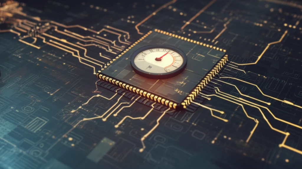
In today's world, where efficiency is key, optimizing power consumption in electronic devices is crucial. Field-Programmable Gate Arrays (FPGAs) offer flexibility, but managing their power usage, especially leakage power, is a significant challenge. This article explores how smart choices in IO standards and dynamic voltage scaling can dramatically reduce energy waste in Vedic multiplier designs implemented on Virtex-6 FPGAs.

Modern FPGAs support a wide array of Input/Output (I/O) standards, each with unique power characteristics. Selecting the right I/O standard can substantially impact the overall energy efficiency of a design. The research detailed here investigates different logic families—LVCMOS, SSTL, and HSTL—to pinpoint the most energy-efficient options for a Vedic multiplier.

Furthermore, dynamic voltage scaling (DVS) offers another avenue for power reduction. By adjusting the supply voltage based on the performance needs of the multiplier, we can minimize power consumption during periods of low activity. This article delves into the combined effects of strategic IO standard selection and DVS, providing insights into optimizing Vedic multiplier designs for minimal leakage power.

Decoding the IO Standard Impact on Power Efficiency

Digital illustration of an energy-efficient Vedic multiplier circuit board.

The choice of IO standard significantly influences the power consumption of FPGA designs. Different logic families, such as LVCMOS (Low Voltage Complementary Metal Oxide Semiconductor), SSTL (Stub Series Terminated Logic), and HSTL (High-Speed Terminated Logic), offer varying levels of power efficiency. Within these families, specific standards further refine power characteristics. For instance, within the LVCMOS family, LVCMOS12 delivers superior power performance, while LVCMOS25 exhibits the worst.

Similarly, HSTL_I_12 stands out as the most power-efficient option within the HSTL family, whereas HSTL_I_DCI_18 consumes the most power. In the SSTL family, SSTL18_I leads in power efficiency, while SSTL2_II_DCI (SSTL2_D) is the least efficient. Understanding these nuances is critical for optimizing power consumption.

Here's a breakdown of the most and least efficient IO standards within each family:
  • LVCMOS Family:
    • Most Efficient: LVCMOS12
    • Least Efficient: LVCMOS25
  • HSTL Family:
    • Most Efficient: HSTL_I_12
    • Least Efficient: HSTL_I_DCI_18
  • SSTL Family:
    • Most Efficient: SSTL18_I
    • Least Efficient: SSTL2_II_DCI (SSTL2_D)
By carefully selecting the most power-efficient IO standards within each family, designers can significantly reduce the overall power consumption of their FPGA-based Vedic multiplier designs. This targeted approach allows for tailored optimization, maximizing performance while minimizing energy waste.

Key Takeaways and Future Directions

This exploration highlights the importance of strategic IO standard selection and dynamic voltage scaling in minimizing power consumption within FPGA-based Vedic multiplier designs. LVCMOS12, HSTL_I_12, and SSTL18_I emerge as the most energy-efficient IO standards within their respective families, offering substantial power savings compared to their less efficient counterparts.

Furthermore, dynamic voltage scaling proves effective in reducing power consumption by adjusting the supply voltage based on performance demands. Combining these techniques offers a comprehensive approach to optimizing Vedic multiplier designs for minimal leakage power and enhanced energy efficiency.

Future research could extend these findings by exploring other IO standards, implementing designs on newer FPGA architectures (e.g., 28nm or 20nm), and integrating these optimized multipliers into larger systems, such as Vedic ALUs or FIR filters. These advancements pave the way for more sustainable and energy-efficient computing solutions across various applications.

About this Article -

This article was crafted using a human-AI hybrid and collaborative approach. AI assisted our team with initial drafting, research insights, identifying key questions, and image generation. Our human editors guided topic selection, defined the angle, structured the content, ensured factual accuracy and relevance, refined the tone, and conducted thorough editing to deliver helpful, high-quality information.See our About page for more information.

This article is based on research published under:

DOI-LINK: 10.17485/ijst/2016/v9i25/96633, Alternate LINK

Title: Leakage Power Reduction With Various Io Standards And Dynamic Voltage Scaling In Vedic Multiplier On Virtex-6 Fpga

Subject: Multidisciplinary

Journal: Indian Journal of Science and Technology

Publisher: Indian Society for Education and Environment

Authors: Bishwajeet Pandey, Md. Atiqur Rahman, Dil M. Akbar Hussain, Abhay Saxena, Bhagwan Das

Published: 2016-07-15

Everything You Need To Know

1

What is dynamic voltage scaling, and how does it reduce power consumption in FPGA-based Vedic multipliers?

Dynamic voltage scaling (DVS) is a technique used to reduce power consumption in electronic circuits. It works by adjusting the supply voltage to the circuit based on its performance requirements at a given time. When the circuit is performing computationally intensive tasks, the voltage is increased to allow for faster operation. During periods of low activity, the voltage is lowered, which significantly reduces power consumption, particularly leakage power. In the context of FPGA-based Vedic multipliers, DVS can be implemented to optimize power usage by reducing the voltage when the multiplier is not operating at its peak performance.

2

How does selecting the right IO standard affect the power consumption in FPGA designs, specifically for Vedic multipliers?

Selecting the appropriate IO standard significantly impacts the power consumption of FPGA designs. Different logic families such as LVCMOS, SSTL, and HSTL offer varying levels of power efficiency. For instance, within the LVCMOS family, LVCMOS12 is more power-efficient compared to LVCMOS25. Similarly, in the HSTL family, HSTL_I_12 consumes less power than HSTL_I_DCI_18, and in the SSTL family, SSTL18_I is more efficient than SSTL2_II_DCI (SSTL2_D). By choosing the most power-efficient IO standards within each family, designers can minimize the overall power consumption of their FPGA-based Vedic multiplier designs.

3

Which IO standards are the most and least energy-efficient within the LVCMOS, HSTL, and SSTL families, and why is this important?

In the LVCMOS family, LVCMOS12 is the most energy-efficient IO standard, while LVCMOS25 is the least efficient. For the HSTL family, HSTL_I_12 offers the best power efficiency, whereas HSTL_I_DCI_18 is the least efficient. Within the SSTL family, SSTL18_I consumes the least power, while SSTL2_II_DCI (SSTL2_D) is the most power-hungry. Selecting the appropriate IO standard based on these differences can significantly reduce the power consumption in FPGA-based Vedic multiplier designs.

4

What is leakage power, and why is it important to minimize it in FPGA designs like Vedic multipliers?

Leakage power is the power consumed by a semiconductor device when it is in an inactive or 'off' state. In FPGA designs, leakage power can contribute significantly to the overall power consumption, especially in advanced technology nodes. Factors contributing to leakage power include subthreshold conduction, gate leakage, and junction leakage. Techniques such as dynamic voltage scaling and the careful selection of IO standards can help reduce leakage power in FPGA-based Vedic multiplier designs.

5

What is a Vedic multiplier, and why is it important to optimize its power consumption when implemented on an FPGA?

A Vedic multiplier is a digital circuit designed to perform multiplication operations using the principles of Vedic mathematics, an ancient Indian system of calculation. Implementing a Vedic multiplier on an FPGA can offer advantages in terms of speed and area efficiency compared to traditional multiplication algorithms. However, like any FPGA design, optimizing power consumption, including leakage power, is crucial. Techniques like dynamic voltage scaling and the strategic selection of IO standards can be applied to minimize power usage in Vedic multiplier designs on FPGAs, enhancing overall efficiency.

Newsletter Subscribe

Subscribe to get the latest articles and insights directly in your inbox.