Gold nanoparticles linked by a molecule between nickel electrodes

Nanogaps for Nanoelectronics: How Self-Assembly is Changing Molecular Devices

"Unlock the Future: Parallel Fabrication Achieves Breakthrough in Molecular Electronic Devices"


In the relentless pursuit of miniaturization and enhanced functionality, single-molecule electronics stands as a beacon, promising to transcend the limitations of current technology. Imagine devices ten times smaller than today's transistors, synthesized in vast quantities, and capable of groundbreaking feats like photoswitching and rectifying behavior. This isn't science fiction; it's the direction in which nanotechnology is headed.

One of the most significant hurdles in realizing single-molecule circuits is the precise positioning of individual molecules within a nanogap, allowing for accurate electronic characterization. Researchers worldwide have been developing innovative platforms, including mechanical break junctions, scanning probe microscopy, and electromigration break junctions, each with its own strengths and limitations.

Now, a compelling alternative is emerging: the protodevice concept. This approach involves isolating single molecules between nanoparticles in a solution and then self-assembling these structures onto prefabricated nanoelectrodes. This method, combined with top-down fabrication techniques, offers a scalable and efficient pathway to create functional molecular electronic devices.

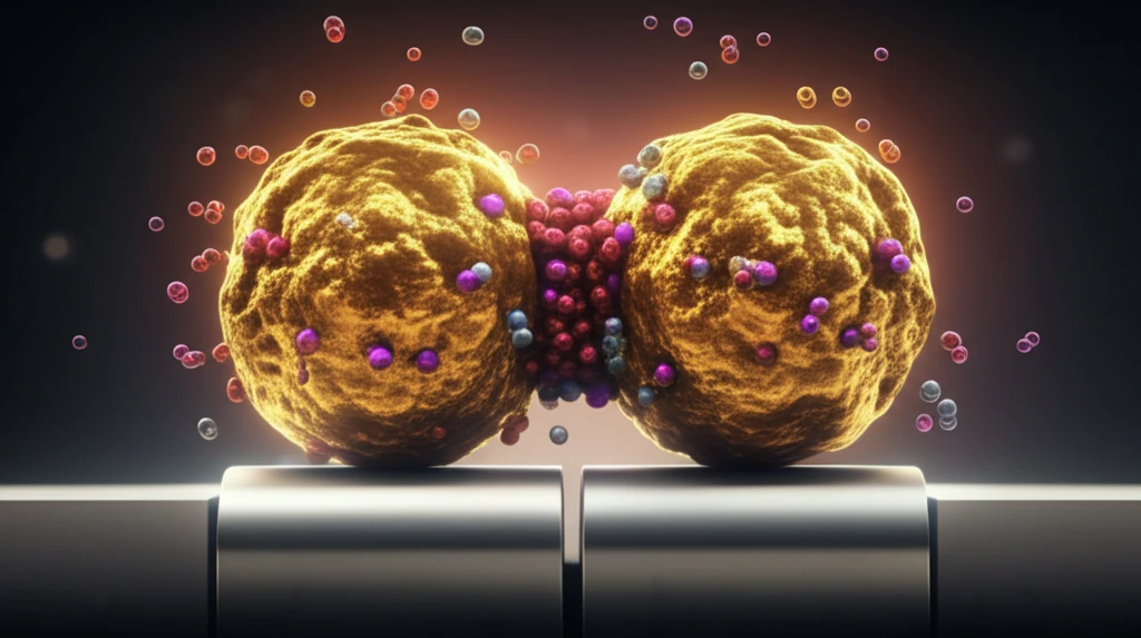
The Science of Self-Assembly: Building Nanogaps with Molecular Precision

Gold nanoparticles linked by a molecule between nickel electrodes

The cornerstone of this innovative approach is the self-assembly of nanogaps, guided by the inherent surface charges of metals and metal oxides in solution. This process leverages a combined top-down and bottom-up strategy, where molecules act as the bridge between two gold nanoparticles, forming a nanogap. These self-assembled nanogaps are then strategically directed onto prefabricated nano-sized nickel electrodes with palladium layers.

The specific geometry of the multilayered metallic electrodes is crucial, carefully optimized to facilitate the assembly of nanostructures through surface charge interactions. This meticulous design ensures an electrode-nanoparticle interface devoid of linking molecules, enabling accurate electrical measurements to probe the electron transport properties of these nanoparticle-molecule-nanoparticle protodevices.

  • Top-Down Meets Bottom-Up: A combined approach for nanoscale assembly.
  • Surface Charge Guidance: Utilizing natural charges for precise placement.
  • Molecule-Free Interface: Ensuring accurate electrical measurements.
Imagine the possibilities: positioning, isolating, and measuring electron transport on single molecules with unprecedented precision. Electron-beam lithography (EBL) plays a pivotal role in fabricating these electrode pairs, optimizing their geometry and materials to encourage the assembly of negatively charged nanoparticle dimers. The electrodes are constructed in layers of nickel (Ni) and palladium (Pd), with nickel attracting citrate-stabilized nanoparticles due to its positive surface potential at pH 6.5–7. The palladium, sandwiched between the nickel layers, enhances conductivity and ensures an oxide-free interface.

What's Next? The Future of Molecular Electronics

The convergence of top-down and bottom-up strategies paves the way for fabricating intricate nanostructures with unparalleled precision. This opens doors to creating complex devices previously unattainable through conventional techniques. By optimizing nanoparticle dimer synthesis and exploring alternative substrates, the efficiency of molecular electronic devices can be substantially improved, ushering in a new era of electronics.

About this Article -

This article was crafted using a human-AI hybrid and collaborative approach. AI assisted our team with initial drafting, research insights, identifying key questions, and image generation. Our human editors guided topic selection, defined the angle, structured the content, ensured factual accuracy and relevance, refined the tone, and conducted thorough editing to deliver helpful, high-quality information.See our About page for more information.

This article is based on research published under:

DOI-LINK: 10.1002/smll.201803471, Alternate LINK

Title: Parallel Fabrication Of Self‐Assembled Nanogaps For Molecular Electronic Devices

Subject: Biomaterials

Journal: Small

Publisher: Wiley

Authors: Johnas Eklöf‐Österberg, Tina Gschneidtner, Behabitu Tebikachew, Samuel Lara‐Avila, Kasper Moth‐Poulsen

Published: 2018-10-25

Everything You Need To Know

1

What is the protodevice concept in the context of single-molecule electronics, and how does it facilitate the creation of functional molecular electronic devices?

The protodevice concept involves isolating single molecules between nanoparticles in a solution. These structures then self-assemble onto prefabricated nanoelectrodes. This approach, in combination with top-down fabrication techniques, offers a scalable and efficient pathway to create functional molecular electronic devices, enabling accurate electronic characterization.

2

How does the self-assembly process of nanogaps work, and what role do surface charges play in guiding this process?

The self-assembly of nanogaps is guided by the inherent surface charges of metals and metal oxides in solution. Specifically, molecules act as the bridge between two gold nanoparticles, forming a nanogap. These self-assembled nanogaps are strategically directed onto prefabricated nano-sized nickel electrodes with palladium layers, leveraging a combined top-down and bottom-up strategy.

3

What is the role of electron-beam lithography (EBL) in fabricating nanoelectrodes, and what materials are used in their construction?

Electron-beam lithography (EBL) is pivotal in fabricating electrode pairs, optimizing their geometry and materials to encourage the assembly of negatively charged nanoparticle dimers. The electrodes are constructed in layers of nickel (Ni) and palladium (Pd), with nickel attracting citrate-stabilized nanoparticles. Palladium, sandwiched between the nickel layers, enhances conductivity and ensures an oxide-free interface.

4

Why is the geometry of multilayered metallic electrodes crucial for the self-assembly of nanostructures, and what is the significance of a molecule-free interface in this process?

The specific geometry of the multilayered metallic electrodes is optimized to facilitate the assembly of nanostructures through surface charge interactions. This meticulous design ensures an electrode-nanoparticle interface devoid of linking molecules, enabling accurate electrical measurements to probe the electron transport properties of these nanoparticle-molecule-nanoparticle protodevices. This molecule-free interface is critical for obtaining accurate electrical measurements.

5

Beyond current achievements, what are the next steps in improving the efficiency of molecular electronic devices using top-down and bottom-up strategies?

By optimizing nanoparticle dimer synthesis and exploring alternative substrates, the efficiency of molecular electronic devices can be substantially improved. Further research is needed in exploring new materials and methods for creating more stable and efficient nanogaps, as well as developing techniques for large-scale production and integration of these devices into existing electronic systems. This includes refining the top-down and bottom-up strategies to improve precision and control over the self-assembly process.

Newsletter Subscribe

Subscribe to get the latest articles and insights directly in your inbox.