
Graphene Nanoribbons: The Staircase to Seamless Electrical Contacts

"Revolutionizing Semiconductor Technology with Atomic Precision"
In the relentless pursuit of more efficient and powerful electronic devices, the quality of electrical contacts is paramount. Traditional metal contacts in low-dimensional semiconductors often introduce unwanted gap states that hinder performance. However, a groundbreaking approach using graphene nanoribbons (GNRs) is set to change the landscape. This method focuses on creating atomically precise heterojunctions, essentially building seamless connections from the atom up.
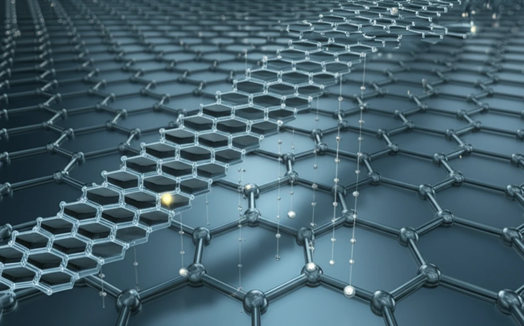
Imagine a staircase, each step a different width of graphene, smoothly transitioning from one material to another. This is the essence of the new technique, which uses all-carbon staircase contacts to connect to semiconducting graphene nanoribbons. These aren't just any connections; they're crafted with such precision that they eliminate the typical interface issues that plague traditional contacts.
The implications of this research are far-reaching, potentially impacting everything from the speed and efficiency of computers to the sensitivity of sensors. By understanding and harnessing the unique properties of graphene at the nanoscale, scientists are opening doors to a new era of electronic devices.
A Conductivity Benchmark 1,000 Times Beyond Copper
Graphene nanoribbons (GNRs) are narrow strips of graphene whose quasi one-dimensional nature yields advantages over the more widely known two-dimensional graphene sheets. In one headline measurement, GNRs tested at Georgia Tech reportedly carried as much as 10 billion amps per square centimeter — nearly 1,000 times the capacity of copper — with researchers noting that no one had measured graphene's current-carrying capacity before this. Sources describe GNRs as an emerging class of one-dimensional materials that host rich quantum-confined and topological states, making them a foundation for quantum electronics. The materials also come in two distinct edge configurations: zig-zag and armchair, with zig-zag ribbons forming at low temperatures and exhibiting spin-polarized metallic edge currents.
From Density-Functional Design to Bottom-Up Synthesis
Standard approaches to GNR electronics pair computational modeling with chemical synthesis: researchers investigate the electronic properties of chemically modified ribbons by means of density functional theory, the method of choice for studying electron transport and gas sensing in armchair GNRs. On the fabrication side, a multistep bottom-up approach has been investigated, and in 2017 dry contact transfer was used to press a fiberglass applicator coated with atomically precise graphene nanoribbons onto a hydrogen-passivated Si(100) surface under vacuum. Other reported synthesis routes include gamma irradiation of graphene and the unzipping of carbon nanotubes. Whatever the fabrication route, the resulting materials are prized for their magnetic properties, which arise from the behavior of unpaired electrons in the atoms' π-orbitals.
It Was Always About the Edges
A foundational insight of GNR research is that the edges matter: in ribbons with zigzag edges, electrons on the two edges display opposite directions of spin — spin-up on one edge and spin-down on the other — an effect illustrated with the precursor molecules used in their manufacture. Historically, GNRs have been framed as counterparts to carbon nanotubes, with advocates highlighting a tunable band gap and a range of electronic properties that carbon nanotubes cannot easily match. A recent milestone reported in Nature Chemistry describes researchers successfully attaching porphyrins to a graphene nanoribbon in a perfectly precise, well-defined manner, creating a so-called 'string light' configuration of periodic edge extensions for tomorrow's electronics.
The Atomic Staircase: How It Works
The core of this innovation lies in the synthesis of coherent heterostructures, which are essentially combinations of GNRs with varying widths. Researchers have successfully created these structures using a surface-assisted self-assembly process, starting with a single molecular precursor. These GNRs consist of 7, 14, 21, and up to 56 carbon atoms across their width, each size offering unique electronic properties.
- Deposition: DBBA molecules are placed on a gold surface.
- Polymerization: Heating to 470K causes the molecules to link.
- Graphitization: Further heating to 670K forms the initial GNRs.
- Conjugation: Annealing at 770K creates the heterojunctions.
A Fast-Moving Field at the Chemical Frontier
Graphene, graphene oxide, and graphene nanoribbons are closely related through their carbon-based planar structures and attractive physical properties, and the chemical synthesis of GNRs has become a central thread of the research literature. Tutorial reviews of this chemistry position bottom-up-synthesized graphene nanoribbons as a powerful platform for next-generation nanoelectronics, spintronics, and quantum technologies thanks to their exceptional electronic properties. Current paper streams remain active, with recent work including first-principles calculations on polarization in graphene nanoribbons with inherent defects. Around these developments, the ongoing news cycle continues to feature new advances in GNR growth and edge engineering.
The Rough Edges of a Promising Material
Not all of the GNR story is triumphant, and sources point to real engineering obstacles. One problem with graphene nanoribbon tunneling field-effect transistors arises from line edge roughness, while the low ON-state current of silicon-based TFETs remains a serious limitation that GNR designs inherit and must overcome. High-power operation is another open question: researchers are investigating the failure limit of graphene nanoribbons under high power loads and trying to find ways to improve it. That work is being conducted as a multi-year effort, with the University at Buffalo leading research expected to span four years.
Topology, Trapped Electrons, and a Path to Silicon Integration
Compared with ordinary semiconductors, GNRs offer capabilities that silicon cannot deliver directly: so-called 'topological' graphene nanoribbons trap electrons in ways that open new quantum materials, a property being explored for next-generation devices. On the integration side, a key comparison involves compatibility with existing chip manufacturing. Researchers at the University of Wisconsin found that thin germanium layers on silicon protected graphene from reacting with silicon while not interfering with the nanoribbons' semiconducting capabilities, an important first step toward creating graphene-based integrated circuits. Together, these threads position GNRs less as a wholesale replacement and more as a specialized platform that must earn its place alongside established silicon processes.
The Future of Electronics: A Seamless Transition
The development of seamless electrical contacts using graphene nanoribbon staircases represents a significant leap forward in semiconductor technology. By creating atomically precise connections, scientists are overcoming the limitations of traditional metal contacts and paving the way for more efficient, powerful, and controllable electronic devices. This innovation holds the potential to revolutionize various fields, from computing and sensors to energy storage and beyond.
Why Graphene Hasn't Taken Over — Yet
Expert commentary around graphene often begins with a candid acknowledgment: despite decades of hype, graphene hasn't taken over the world yet, and turning extraordinary lab results into deployed technology remains the central challenge. Within that larger story, graphene nanoribbons are positioned as the more tractable piece of the puzzle — narrow strips of graphene whose quasi one-dimensional nature delivers additional advantages over the two-dimensional sheets that first captured public attention. The practical question, as commentators frame it, is whether the production and integration hurdles can be overcome so that these advantages translate from the benchtop to the fab line.
Alignment on Germanium and a Market Poised for Growth
Growth reports project that the graphene nanoribbons market is positioned for exponential growth from 2026 to 2033, driven by technological breakthroughs, expanding application horizons, and supportive policy frameworks. On the technical side, researchers discovered that graphene nanoribbons grown on germanium automatically align perpendicularly and naturally form in the armchair edge configuration, an advance that could enable faster, more efficient electronics. In a separate breakthrough, chemists successfully produced graphene nanoribbons directly on semiconductor surfaces, simplifying production and offering the ability to customize the nanoribbons' properties. That direct-on-semiconductor capability points toward practical applications, including in storage technology.
Surviving the Extremes: From Fusion Reactors to Atom-Precise Tuning
The systemic challenge for GNRs is proving themselves in extreme, real-world environments, not just in controlled lab settings. A US study showcased graphene nanoribbons that can withstand extreme conditions, suggesting GNR-based sensors could eventually be engineered to operate closer to fusion reactors. At the other end of the spectrum, researchers are learning to tune spin and charge with atomic precision: an insulating magnesium oxide layer decouples the graphene nanoribbon from a metal's electronic sea while still letting electrons move between them in quantized amounts — one by one, rather than continuously. Together these results sketch a material that must handle both punishing environments and exquisitely delicate quantum control.
First Light From a Single Ribbon
Some of the most humanly resonant results are the visible ones: for the first time, scientists observed light emitting from individual graphene nanoribbons — strips narrower than 50 nanometers known for their highly tunable band gaps — with the ribbons emitting an estimated 10 million photons per second. Such emission measurements turn a nanoscale material into something observable and countable, bridging the gap between abstract quantum physics and tangible phenomena. Alongside these optics breakthroughs, researchers continue deep theoretical work, including quantum Monte Carlo studies of magnetic correlation in graphene. The combined effort reflects a field where fundamental theory and single-ribbon experiments advance together toward practical impact.