Glowing zinc oxide nanowires on silicon wafer with seed layers

Future Tech: How 'Seeded' Nanowires Could Revolutionize Electronics

"Scientists explore how seed layers influence the growth of iron-doped zinc oxide nanowires, paving the way for enhanced electronic components."


In the relentless pursuit of technological advancement, materials science stands as a pivotal force, constantly pushing the boundaries of what's possible. Nanomaterials, with their unique properties, are at the forefront of this revolution, promising to transform industries from electronics to medicine. Among these, zinc oxide (ZnO) nanowires have garnered significant attention due to their potential in creating more efficient and versatile devices.

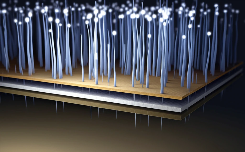
A recent study has shed light on a novel approach to enhance the growth and characteristics of ZnO nanowires by using 'seed layers' of aluminum (Al) and titanium (Ti). This innovative technique involves depositing a thin layer of these metals onto a silicon substrate before growing the ZnO nanowires. The presence of these seed layers significantly influences the resulting structure and properties of the nanowires, opening up new avenues for tailoring materials at the nanoscale.

This article delves into the fascinating world of materials science, exploring how the strategic use of seed layers can optimize the growth of ZnO nanowires. We'll unpack the science behind this method, discuss the implications of this research, and consider how these advancements might shape the future of technology. Whether you're a tech enthusiast, a science student, or simply curious about the innovations that will define tomorrow, this exploration of seeded nanowires promises to be both enlightening and inspiring.

Unlocking Nanowire Potential: The Role of Seed Layers

Glowing zinc oxide nanowires on silicon wafer with seed layers

The focus of the research is on understanding how different seed layers impact the growth of zinc oxide (ZnO) nanowires. These nanowires are not just any ordinary material; they're engineered at an incredibly tiny scale, measured in nanometers (billionths of a meter). Their size gives them unique electrical and optical properties, making them ideal for use in advanced electronic devices.

The scientists grew ZnO nanowires on silicon (Si) substrates using a technique called electron beam evaporation. However, before growing the nanowires, they deposited thin layers, or 'seed layers,' of either aluminum (Al) or titanium (Ti) on the silicon. These seed layers act as a foundation upon which the nanowires grow. The choice of seed layer can dramatically affect the final structure and behavior of the nanowires.

  • Aluminum (Al): Known for its excellent electrical conductivity and ability to form stable oxides.
  • Titanium (Ti): Offers high strength, low density, and resistance to corrosion.
The researchers also introduced iron (Fe) doping into some of the ZnO nanowires. Doping involves adding a small amount of another element to a material to alter its properties. In this case, iron doping can change the electrical and magnetic characteristics of the ZnO, making it suitable for specialized applications.

The Future is Nano: Promising Applications and Beyond

The exploration of seed layers and their impact on nanowire growth represents a significant stride in materials science. By understanding and controlling these fundamental processes, scientists are paving the way for the development of advanced electronic devices with enhanced performance and versatility. From improved sensors to more efficient energy technologies, the potential applications are vast and transformative. As research in this field continues, we can anticipate even more exciting innovations that will shape the future of technology.

About this Article -

This article was crafted using a human-AI hybrid and collaborative approach. AI assisted our team with initial drafting, research insights, identifying key questions, and image generation. Our human editors guided topic selection, defined the angle, structured the content, ensured factual accuracy and relevance, refined the tone, and conducted thorough editing to deliver helpful, high-quality information.See our About page for more information.

This article is based on research published under:

DOI-LINK: 10.1016/j.mssp.2017.08.015, Alternate LINK

Title: Effect Of Seed Layers (Al, Ti) On Optical And Morphology Of Fe-Doped Zno Thin Film Nanowires Grown On Si Substrate Via Electron Beam Evaporation

Subject: Mechanical Engineering

Journal: Materials Science in Semiconductor Processing

Publisher: Elsevier BV

Authors: I. Neelakanta Reddy, Ch.Venkata Reddy, M. Sreedhar, Migyung Cho, Jaesool Shim, V. Rajagopal Reddy, Chel-Jong Choi, Dongseob Kim

Published: 2017-11-01

Everything You Need To Know

1

How do aluminum and titanium seed layers affect the growth of zinc oxide nanowires?

The study uses seed layers of aluminum (Al) and titanium (Ti) on silicon substrates to influence the growth of zinc oxide (ZnO) nanowires. Aluminum is known for its electrical conductivity, and titanium offers high strength and corrosion resistance. These seed layers act as a foundation, affecting the structure and behavior of the nanowires, which is crucial for tailoring materials at the nanoscale for specific electronic applications.

2

What is iron doping and how does it modify the properties of zinc oxide nanowires?

Iron (Fe) doping involves adding a small amount of iron to zinc oxide (ZnO) nanowires to alter their electrical and magnetic properties. This doping process allows scientists to customize the nanowires for specialized applications by enhancing specific characteristics that are crucial for advanced electronic devices.

3

Why are zinc oxide nanowires considered promising materials for future technologies?

Zinc oxide (ZnO) nanowires show promise in several fields because of their unique electrical and optical properties stemming from their nanoscale size. This makes them suitable for advanced electronic devices, sensors, and energy technologies, where efficiency and versatility are highly valued.

4

What is electron beam evaporation and how does it facilitate the growth of zinc oxide nanowires with controlled properties?

Electron beam evaporation is used to grow zinc oxide (ZnO) nanowires on silicon (Si) substrates. This method involves depositing thin layers of aluminum (Al) or titanium (Ti) as seed layers before the nanowires are grown. This technique allows for precise control over the nanowire's growth and properties, which is essential for creating high-performance electronic components. Other methods such as sputtering, chemical vapor deposition, or pulsed laser deposition could also be employed, each offering its advantages in controlling film properties and growth rates, which could lead to different nanowire characteristics and device performance.

5

What are the broader implications of using seed layers to control the growth of zinc oxide nanowires for technological advancement?

The exploration of seed layers, such as aluminum (Al) and titanium (Ti), to control the growth of zinc oxide (ZnO) nanowires has significant implications for the advancement of technology. By tailoring the properties of these nanowires, scientists can develop more efficient and versatile electronic devices. This impacts not only electronics but also areas like sensors and energy technologies, promising advancements that can reshape various aspects of our daily lives and industries.

Newsletter Subscribe

Subscribe to get the latest articles and insights directly in your inbox.