Nanoscale electron emitters revolutionizing technology.

Tiny Titans of Tech: How Nanoscale Electron Emitters Are Revolutionizing Modern Technology

"Unlocking the potential of cold field electron emission for brighter displays, sharper microscopes, and beyond."


In today's rapidly advancing technological landscape, breakthroughs often come in the smallest of packages. Cold Field Emission (CFE), a process involving the emission of electrons from a material under the influence of a strong electric field, is one such innovation. Contributing significantly to technologies like electron microscopes and field-emission displays, CFE is also pivotal in the evolution of vacuum nanoelectronics and even impacts our understanding—and prevention—of vacuum breakdowns. But what makes CFE so compelling, and how is it reshaping the future of technology?

At its core, CFE offers a unique way to generate electron beams without relying on high temperatures. This is particularly important because it allows for more precise control and energy efficiency, crucial for applications requiring high resolution and minimal thermal disturbance. The underlying theory, rooted in Fowler-Nordheim (FN) tunneling, allows electrons to escape from the surface of a material when an electric field is applied. The key to understanding and optimizing this process lies in the careful characterization of the materials and their emitting surfaces.

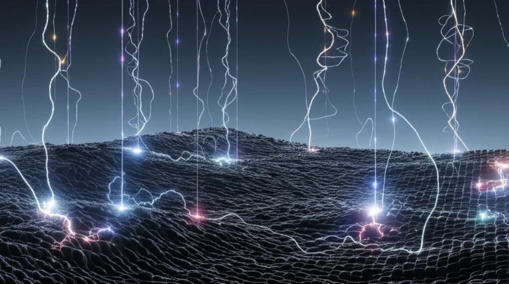
One critical parameter in CFE is the emitting surface area, which directly impacts the lifespan and stability of electron sources. Recently, it's been discovered that the notional area of emission—the effective area from which electrons appear to originate—plays a crucial role, especially in emitters with larger diameters. This realization has sparked a need to deeply understand how this notional area depends on various physical and geometrical parameters. This article dives into the groundbreaking research analyzing how these parameters affect the efficiency and brightness of CFE arrays.

Understanding the Notional Area in Cold Field Emission

Nanoscale electron emitters revolutionizing technology.

Recent studies, like the one from Amorim et al. (2018), focus on unraveling the complexities of the notional area (An) in CFE, particularly within arrays of emitters. These arrays, often modeled as a hemisphere on a cylindrical post (HCP), are suitable for simulating carbon nanotubes or nanofiber-like emitters. The aim is to determine how An is affected by key factors such as the separation between emitters, aspect ratio, radius, local work function, and macroscopic emission current. This kind of deep dive provides insights into maximizing the performance of electron sources.

The researchers used extensive numerical simulations to evaluate An under various conditions, revealing that its behavior is influenced by a combination of physical and geometrical parameters. Understanding these relationships allows scientists and engineers to optimize the design of CFE arrays for specific applications. Here are some important areas explored:

  • Emitter Spacing: The distance between HCP emitters significantly impacts the electric field distribution and, consequently, the notional area.
  • Aspect Ratio: The height-to-radius ratio of the emitters influences the concentration of the electric field at the tip.
  • Local Work Function: The energy required for an electron to escape the material’s surface affects the emission efficiency.
  • Emission Current: The macroscopic emission current dictates the overall performance of the electron source.
Ultimately, the goal is to simplify the modeling of field emission phenomena by directly linking simulation predictions to experimentally observable currents. By understanding the interplay between these parameters, experimentalists can better validate models like the Schottky-Nordheim (SN) barrier, which describes the energy barrier electrons must overcome to be emitted. These detailed analyses are essential for refining CFE technology and making it more reliable and efficient.

Future Implications and Applications

The ongoing research into cold field emission and the optimization of notional emission areas promises exciting advancements across various fields. Improved electron microscopes can offer unprecedented resolution for scientific research, while more efficient field-emission displays could lead to brighter, more energy-efficient screens. As nanotechnology continues to evolve, the potential applications for optimized CFE sources are virtually limitless. By pushing the boundaries of what’s possible at the nanoscale, we’re paving the way for a future where even the tiniest components can have a massive impact.

About this Article -

This article was crafted using a human-AI hybrid and collaborative approach. AI assisted our team with initial drafting, research insights, identifying key questions, and image generation. Our human editors guided topic selection, defined the angle, structured the content, ensured factual accuracy and relevance, refined the tone, and conducted thorough editing to deliver helpful, high-quality information.See our About page for more information.

This article is based on research published under:

DOI-LINK: 10.1088/1361-648x/aadbdf, Alternate LINK

Title: Numerical Analysis Of The Notional Area In Cold Field Electron Emission From Arrays

Subject: Condensed Matter Physics

Journal: Journal of Physics: Condensed Matter

Publisher: IOP Publishing

Authors: Mauro V Amorim, Fernando F Dall’Agnol, Daniel Den Engelsen, Thiago A De Assis, Vitor Baranauskas

Published: 2018-08-30

Everything You Need To Know

1

What is Cold Field Emission (CFE), and how does it differ from traditional electron emission methods?

Cold Field Emission (CFE) works by applying a strong electric field to a material, causing electrons to be emitted. This process relies on Fowler-Nordheim (FN) tunneling, where electrons escape the material's surface due to the electric field, without needing high temperatures. This is highly advantageous because it enables precise control and greater energy efficiency, essential for applications demanding high resolution and minimal thermal disturbance. Unlike traditional methods that rely on heat, CFE offers a 'cold' electron source, reducing thermal effects and improving the performance of devices like electron microscopes and field-emission displays.

2

What is the "notional area" (An) in the context of Cold Field Emission (CFE), and why is it important?

The notional area (An) in Cold Field Emission (CFE) refers to the effective area from which electrons appear to originate during emission. It is influenced by several factors, including the emitter spacing, aspect ratio (height-to-radius ratio), local work function, and the macroscopic emission current. Understanding and optimizing the notional area is crucial for improving the lifespan, stability, and overall performance of electron sources, particularly in cold field emission arrays. Research, such as the study by Amorim et al. (2018), focuses on how these parameters collectively affect the efficiency of CFE arrays, typically modeled using structures like a hemisphere on a cylindrical post (HCP).

3

What are the key factors that influence the "notional area" (An) in Cold Field Emission (CFE) arrays?

Key factors influencing the notional area (An) in Cold Field Emission (CFE) arrays include emitter spacing, aspect ratio, local work function, and macroscopic emission current. Emitter spacing affects the electric field distribution, the aspect ratio influences the electric field concentration at the emitter tip, the local work function determines the energy required for electrons to escape, and the emission current dictates the overall electron source performance. The interplay of these parameters defines the notional area's characteristics and is essential for optimizing the design and performance of CFE arrays. By fine-tuning these parameters, engineers can maximize the efficiency and stability of electron emission.

4

How do advancements in Cold Field Emission (CFE) technology impact applications like electron microscopes and field-emission displays?

Advancements in Cold Field Emission (CFE) technology have significant implications for electron microscopes and field-emission displays. Improved electron microscopes could achieve unprecedented resolution, enhancing scientific research capabilities. More efficient field-emission displays could lead to brighter, more energy-efficient screens for various devices. These improvements stem from a better understanding and optimization of parameters such as the notional area, emitter spacing, and material work function. Furthermore, the ongoing research contributes to refining models like the Schottky-Nordheim (SN) barrier, leading to more reliable and efficient CFE technology applicable across diverse nanoscale applications.

5

What is the significance of the Schottky-Nordheim (SN) barrier in understanding and optimizing Cold Field Emission (CFE)?

The Schottky-Nordheim (SN) barrier is an energy barrier that electrons must overcome to be emitted from a material's surface in Cold Field Emission (CFE). The SN model helps describe and predict the emission behavior based on material properties and applied electric fields. Experimentalists validate the SN model by comparing simulation predictions with experimentally observed currents, ensuring that the theoretical models accurately reflect real-world performance. Refining and validating the SN barrier model is crucial for enhancing the reliability and efficiency of CFE technology, allowing for more precise control and optimization of electron emission in various applications.

Newsletter Subscribe

Subscribe to get the latest articles and insights directly in your inbox.