
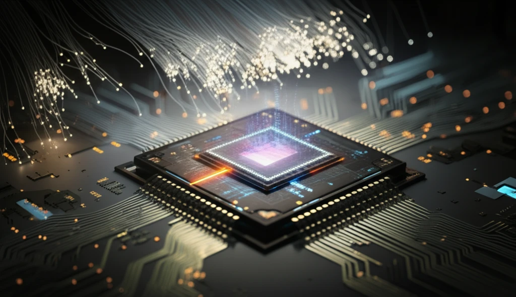
Silicon Breakthrough: How New Chip Designs Could Revolutionize Your Tech

"Researchers are making waves with III-V semiconductors integrated on silicon, paving the way for faster, more efficient devices."
Imagine a world where your devices are not only faster but also consume significantly less power. This vision is rapidly becoming a reality thanks to groundbreaking advancements in silicon photonics. As the demand for increased network capacity continues to surge globally, researchers are tirelessly working to push the boundaries of what's possible with silicon, aiming to create more efficient and cost-effective solutions for optical transceivers.
Silicon photonics has emerged as a promising platform due to its potential for mass production using well-established CMOS-compatible fabrication technology. Traditionally, silicon has been a key material in creating Mach-Zehnder modulators, germanium photodetectors, and compact waveguide optical filters. However, silicon alone has limitations, particularly in applications like laser diodes where its indirect bandgap presents challenges.
To overcome these hurdles, scientists are exploring heterogeneous integration—combining different materials with silicon to enhance its capabilities. One exciting approach involves integrating III-V semiconductors onto silicon platforms using direct wafer bonding methods. These semiconductors offer direct bandgaps and significant carrier-induced refractive index changes, making them ideal for laser diodes and Mach-Zehnder modulators. The result? Devices with improved performance and reduced power consumption.
Silicon's Scale and Computing Role
Silicon is the second most abundant element in Earth's crust, making up 27.7 percent of it, according to Britannica. It is widely distributed in space and on planets mainly as silicon dioxide or silicates, while pure silicon is rare in Earth's crust. As a semiconductor, silicon is used extensively in computers, and a typical desktop computer contains several dozen integrated circuits made mostly of silicon. Research involving silicon-28, which can now be made 40 times purer than before, may support future computer developments involving qubits embedded in atoms such as phosphorus.
Established Silicon Methods
Conventional chip development generally relies on silicon semiconductor technology and integrated circuits. This approach has enabled widespread computer production, but its established methods may face limitations as designers seek further gains in computing capability, efficiency, and miniaturization. Without specific source evidence here, the precise nature and scale of those limitations should be treated cautiously.
Silicon's Foundations
Silicon's importance to modern technology developed through its use as a semiconductor and material for integrated circuits. Its role expanded as computers incorporated many silicon-based circuits into a single desktop system. The supplied material does not establish a detailed timeline of discoveries or milestones, so broader historical claims require additional sourcing.
Why Combining III-V Semiconductors with Silicon Is a Game-Changer
The integration of III-V semiconductors with silicon addresses some critical limitations of using silicon alone, especially in laser diodes. Silicon and germanium's indirect bandgaps make them less efficient for light emission, necessitating external laser diode modules that add to the cost and complexity of devices. By heterogeneously integrating III-V materials, which possess direct bandgaps, researchers can create more efficient and compact laser diodes directly on the silicon platform.
- Enhanced Laser Performance: Direct bandgap materials improve light emission efficiency.
- Improved Modulation Efficiency: Larger refractive index changes reduce size and power needs.
- Versatile Wavelength Filtering: Silicon oxide films offer tailored refractive indices.
Research Directions
Current discussion of chip innovation includes efforts to extend silicon's capabilities beyond conventional computing. The supplied material points specifically to highly purified silicon-28 and its potential importance for future computer development involving qubits in phosphorus-containing systems. Because no detailed research review was provided, the maturity, performance, and timeline of this direction remain uncertain.
Limits and Lessons
Silicon's technological importance does not remove the need to examine its limitations and the challenges involved in advancing chip designs. The supplied source reports that silicon was discovered in 1823 by Jöns Jacob Berzelius and identifies it as the second most abundant element in Earth's crust. That historical and material abundance alone does not demonstrate that every proposed silicon-based breakthrough will succeed.
Comparing Chip Approaches
Silicon remains the established reference point for semiconductor computing because it is widely used in computers and integrated circuits. New chip approaches can therefore be evaluated by whether they improve on silicon's computing performance, efficiency, or future scalability. The available material does not provide comparable measurements or competing technologies, so no specific ranking can be justified.
The Future of Silicon Photonics: A Glimpse into Tomorrow's Tech
The advancements in integrating III-V semiconductors with silicon photonics are paving the way for a new era of high-performance, low-cost optical transceivers. As research continues and these technologies mature, we can expect to see widespread adoption in various applications, from data centers to consumer electronics. The promise of smaller, faster, and more energy-efficient devices is no longer a distant dream but a tangible reality on the horizon.
A Silicon-Based Synthesis
The supplied evidence presents silicon as both an abundant crustal element and a central semiconductor material in modern computers. It also identifies silicon-28 purification and qubit-related applications as a possible direction for future computer development. These points support cautious optimism, but the material does not establish that such research will produce a commercial breakthrough.
The Next Silicon Frontier
One possible frontier is the use of highly purified silicon-28 in computing systems that store qubits in atoms such as phosphorus. The supplied material reports that silicon-28 can now be made 40 times purer than before and describes this as important for the next major development in computers. It does not provide a deployment date, performance projection, or evidence that the approach has reached widespread use.
Scale, Supply, and Complexity
Silicon's broad distribution in the Earth's crust and throughout space contrasts with the difficulty of producing it in the specialized forms required by advanced computing. The supplied material distinguishes silicon's abundance from the rarity of its pure form in Earth's crust. It does not document particular supply-chain, environmental, manufacturing, or policy challenges, so those issues cannot be assessed specifically here.
Silicon in Everyday Computing
Silicon already affects everyday life through the integrated circuits found in typical desktop computers. The supplied material reports that such a computer contains several dozen integrated circuits made mostly of silicon. Future silicon-based developments could influence computing, but the available sources do not establish specific effects on users, jobs, access, or society.